Starting up with Xilinx ISE
I personally found the initial project wizard quite a bit cumbersome, specially considering it asks lots of questions with sparse documentation. Also missing is a what to do now kind of welcome screen, specially if you don’t come from a heavy Xilinx tools background, and just want to toy with your little Verilog program in the development kit.
So here’s what I usually do create a new project in ISE these days. We’ll assume that you installed ISE in /opt/xilinx; if you installed it somewhere else you’ll have to use the appropriate absolute paths everywhere.
-
Open a Terminal and source the right environment variables (PATH, library paths, etc.) from your ISE installation.
If you’re using a 32 bit operating system and Bash,
source /opt/xilinx/ISE_DS/settings32.sh. If you’re using a 64 bit kernel and Bash,source /opt/xilinx/ISE_DS/settings64.shIf using a csh-like shell, replaceshwithcsh. -
Now start ISE by running
ise. -
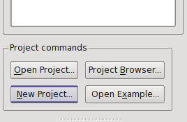
An empty workspace should appear (if it doesn’t you can click File -> Close project). Select “New project” from the left pane to begin.
-
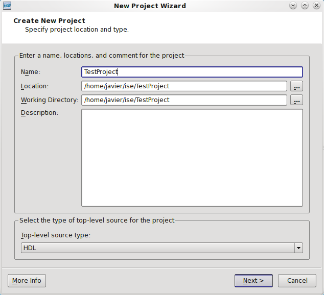
The New project wizard’s first question is trivial: your project’s name. Also asked is your project’s type: HDL means a VHDL or Verilog project.
-
Next question involves having the target hardware readily at hand. Basically, you have to enter the FPGA exact model. Sometimes it’s written on the FPGA chip itself:
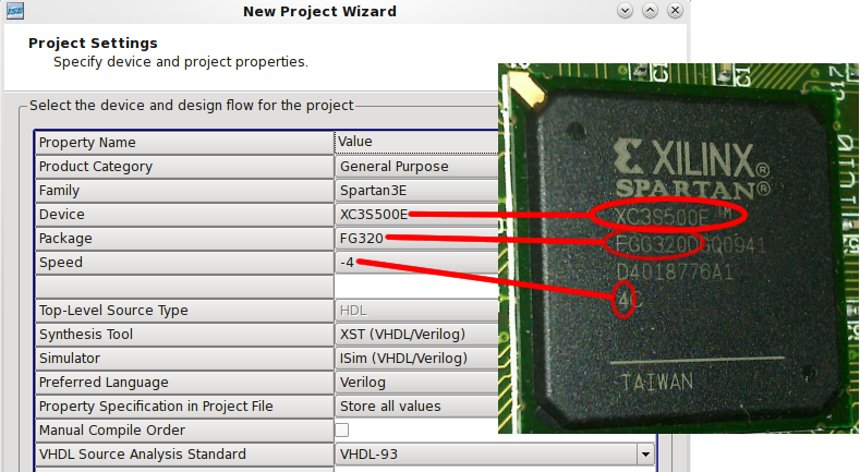
This was from a Spartan 3E Starter kit. For some other kits, you will have to look up the manual. For example, settings for a XUPV5-LX110T evaluation board:
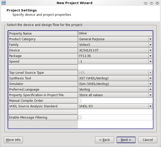
Also ensure you select Verilog as your preferred language.
-
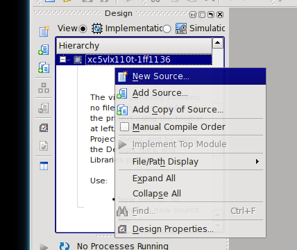
Right after the obligatory confirmation dialog, your project will be created, and you will enter “Implementation mode”. Next step is to create the “root” module, or the one whose ports will be mapped to the FPGA’s physical pins. ISE will automatically try to guess which one of all the Verilog modules is your design’s root module – the one not instanced by any other module – so try to follow that rule. To create a new Verilog module, right click on the project icon in the project explorer:
-
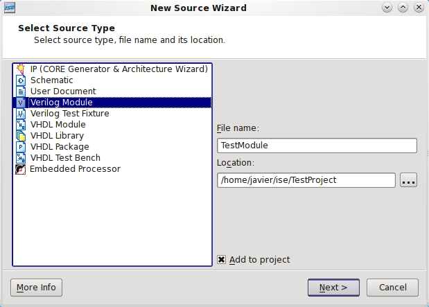
Select “Verilog Module” and name it as you wish.
-
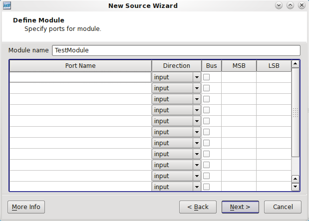
The following dialog will just ask for the ports the module will have as a convenience. If you do fill them in the table here, ISE will fill the Verilog module declaration for you; if you don’t, you will have to write it later. Since typing them in Verilog might actually be faster than using the GUI, I suggest skipping this altogether and pressing Next.
-
The text editor opens with your newly created .v file. For a start, I’m going to write the following trivial program:
 module TestModule(
         input gpio_sw_c,
         output gpio_led_c
     );

     assign gpio_led_c = !gpio_sw_c;

 endmodule
Note the port names. Root module <-> FPGA pin mappings are done by name (in a case insensitive manner), so getting them right is quite important.
-
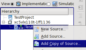
This list of names comes from what is called a Implementation Constrains file (or .ucf file). This file maps FPGA pins to “port names”, and might also add some extra information per pin like the desired voltage level). Obviously, the contents of this file depend on your board’s configuration. I’ve uploaded UCF files for the Spartan 3E and the XUPv5-LX110T boards. You have to download the corresponding UCF file (possibly from your dev board’s website), and add it to the project:
-
If you take a look at the newly added file, you’ll see that every line is prefixed with # (so, every line is commented out). You have to uncomment the pins you plan to use, and only those; if you add more pins that you use in your root module the synthesizer will complain. For the above example, look for the
GPIO_SW_CandGPIO_LED_Clines, and remove the prefixing # from them. -
So, we have the UCF file and the root module; this simple design is complete. Now we need to synthesize it and upload it to our board. If you click on your root module in the left pane, the bottom part of it will change to show the Processes view.
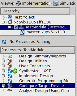
This is like a Makefile, only with each of its targets shown visually on a list, ordered so that each one depends on the previous ones only. Double clicking on a “target” will automatically build it and all its prerequisites, so double clicking on Configure Target Device will automatically start the synthesis process and try to program your board.
-
After the synthesis and implementation processes end, however, you will see a warning (No IMPACT project file found), since ISE doesn’t know how to program the board. For example, which of the devices available on your board should it configure: the FPGA chip which remember, will lose its configuration after removing power from the board or the Flash chip, which won’t. This is all decided using the IMPACT program, which will open as soon as you dismiss the warning.
-
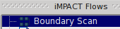
On IMPACT, double click on Boundary Scan.
-
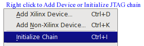
Right click on the blank area that opens and select Initialize Chain. It’s a good idea to have the board powered on and plugged in by now :).
-
If everything went well (and if it didn’t, you should check up on the USB cable), a set of chip icons representing each of the found devices will appear in IMPACT, and it will ask you whether autoassign configuration files. I usually say No here, as it will try to assign a file for each chip available, but I usually want to program a single chip instead.
-
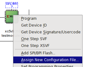
Right click on your FPGA “chip” icon (identified by model e.g. xc5vlx110t, or XC3S500E), and select “Assign New Configuration File…”.
-
Browse to your project folder and select the only .bit file available there. This is the output of the “Generate Programming File” target in ISE, which was run as a prerequisite in step 12.
-
Right click again on the FPGA and select “Set Target Device”, as this is the device we want to program.
-
Right click again, and select “Program”! It will ask whether you want to verify what’s been programmed, I usually leave it unchecked.
If this quite simple design for the XUPV5 worked, you should check whether holding the centre button shuts the centre LED off.
Now, you’ll most probably want to go back to editing your constraints / UCF file, to enable additional pins from your board; remember that you’ll have to edit your root module ports appropriately too.
If you don’t want to be asked about IMPACT every time you double click on “Configure target device”, you should Save your IMPACT project now (somewhere within the ISE project root folder) and then right click on the “Configure target device” process in ISE, setting the “IMPACT Project File” setting to the file you previously saved. From then one, ISE will program the board as you told IMPACT without asking you.
Note that it might take a while and there won’t be ANY progress feedback at all while ISE does it.